New Possibilities for Live Cell Imaging & Semiconductor Inspection with Hyperspectral Microscopy
By Mike Fussell, Life Sciences Product Manager
Published on May 24, 2024
While fluorescence microscopy has traditionally been focused on the visible spectrum, the advent of digital cameras sensitive to wavelengths beyond the visible spectrum has opened up a range of possibilities in the ultraviolet and infrared range.
This article introduces uses of hyperspectral microscopy and provides guidance on the selection of objectives and cameras to achieve the best possible results.
Near Infrared (NIR) Microscopy for Live Cell Imaging
Protect your live cells, simplify your experimental design and gather more accurate data with Near Infrared (NIR) and Shortwave (SWIR) microscopy. Lower energy, longer wavelength IR photons are less cytotoxic than shorter wavelength, higher energy photons in the visible and UV bands of the spectrum. By avoiding unwanted phototoxicity, cells can be studied for longer. NIR microscopy can save time, cost and complexity by eliminating the need for complex genetically encoded bioluminescent reporters like luciferase in many live cell studies.
Experimental Design Tip: NIR imaging can be used in conjunction with calcium imaging, provided that the longer emission wavelength calmodulin reporters are used.
Selecting the Right Optics for NIR Microscopy
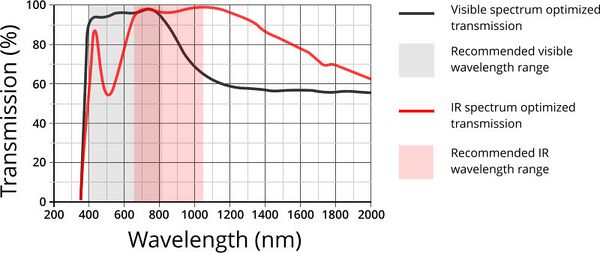
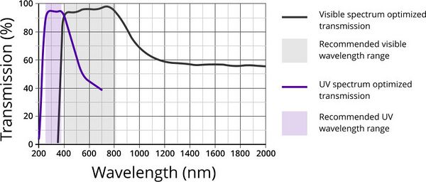
To ensure the best performance, IR-optimized objectives should be used. Check the transmission plot (fig. 2) of the objective in its datasheet to ensure the wavelengths you intended to use will transmit an adequate amount of light. The low intensity of Fluorescence signals means that even a small decrease in objective transmission efficiency will have a direct impact on the duration of the exposure required to reliably detect it. Longer exposure times translate into reduced throughput.
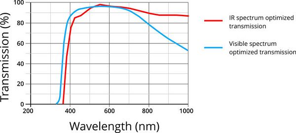
Manufacturers may also make specific recommendations of the nominal wavelength range of objectives. While an objective may have acceptable transmission for a wavelength of interest, it may not focus well or may produce unwanted chromatic aberrations if it is used outside its intended range.
In addition to objectives, the NIR performance of a microscope will also be dictated by its tube lens. In many microscope systems, replacing optical components can be costly and complex - if it is even possible. Zaber’s Nucleus® modular microscope platform makes it easy to get started with NIR imaging. Installing an NIR tube lens takes less than a minute! Likewise, NIR illumination can be added to the system in less than two minutes. Illuminator modules with the LED wavelengths of your choice are available upon request.
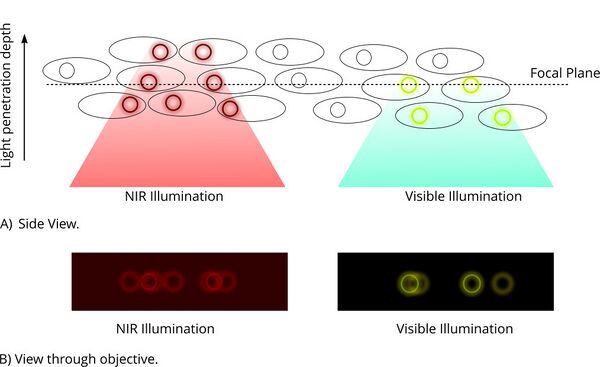
As the amount of tissue between the sample surface and the focal plane increases, the amount of out of focus fluorophores which are excited increases too. The light from these out of focus fluorophores can create a haze which may make it difficult to identify weak signals. AI processing tools like those available in Viziview can help to remove the haze and improve the signal to noise ratio.
Camera Selection for NIR Microscopy
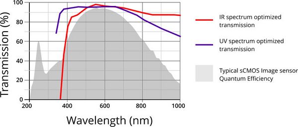
CMOS and CCD camera performance is wavelength dependent. The % of incoming photons which successfully knock electrons off silicon atoms in the image sensor’s photodiode is referred to as Quantum Efficiency (QE). At longer wavelengths beyond 850 nm the efficiency of most CMOS image sensors will be < 50% (fig. 3).
This will necessitate longer exposures and/or higher sensor gain to capture images in equivalent brightness to fluorophores which emit light at wavelengths closer to your camera’s peak QE. This Zaber article provides a more in-depth discussion on camera selection for microscopy.
Special Considerations for NIR Microscopy
The maximum spatial resolution of your images in the XY plane will decrease as the wavelengths you are working with increase in length. This relationship is described by Abbe’s diffraction limited resolution formula: d = λ/(2NA)
The diffraction limited Spatial resolution in the lateral plane is equal to the wavelength divided by two times the numerical aperture. An in-depth discussion of the advantages and disadvantages of different numerical aperture lenses is beyond the scope of this article. However, in general, higher numerical aperture objectives will yield improved spatial resolution and capture more light leading to brighter images. Higher numerical aperture lenses will have shallower depth of field which may or may not be an advantage depending on the application.
The long excitation wavelength and even longer emission wavelengths for (NIR) fluorophores like Cy7 penetrate more deeply into tissues, enabling fluorescent microscopy of cells in a more natural microenvironment. Deeper penetration may, however, result in decreased signal to noise ratio.
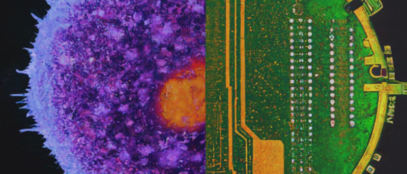
NIR and SWIR Microscopy for Semiconductor Inspection
NIR and SWIR wavelengths will also penetrate more deeply into silicon substrates making NIR microscopy a useful tool for semiconductor development and inspection. Advancements in packing and die stacking are driving the development of advanced chiplet-based designs which introduce possible sub-surface defects like misaligned through silicon vias (TSVs) and cracking caused by the stress of packaging. IR microscopy can be employed to detect these defects.
Ultraviolet (UV) Microscopy for Increased Resolution
Resolve finer details with UV microscopy. The increased spatial resolution which can be achieved with UV imaging is ideal for semiconductor and surface inspection applications where fine details are critical and phototoxicity is not an issue. The shorter wavelengths in the UV portion of the spectrum allow for higher spatial resolution than longer visible and IR wavelengths. This is the inverse of the phenomenon observed in IR wavelengths described above. UV microscopy is also frequently used in pharmaceutical applications for measuring the dispersal of active ingredients in formulations and the identification of potential contaminants.
Special Considerations for UV Microscopy
UV microscopy has many of the same caveats as NIR microscopy. As with NIR microscopy, specialized objectives are required with optical materials and coatings optimized for the transmission of short wavelengths. UV optimized objectives usually have the term Fluor or Fluar in their names. For example, Nikon’s CFI Plan Fluor series.
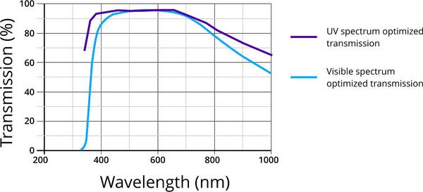
Optimizing a microscope to perform well in the UV range is more demanding than for NIR. UV-optimized tube lenses, illuminators and cameras require more exotic optical materials and coatings than for NIR-optimized systems. This is reflected in the cost of these components. For example, a high quality Mitutoyo 50X objective optimized for visible spectrum imaging will cost about $3,500 USD, whereas a UV optimized objective with the same magnification and numerical aperture will cost about $18,000 USD.
High energy UV photons can be damaging to biological materials. UV imaging is not recommended for live cell imaging due to its phototoxic effects. Other biological materials which can be damaged by UV light include human eyes. Best-practices for eye safety should always be observed when working with a UV microscope. Do not look directly at a UV illuminated sample without proper eye protection! UV illumination can also degrade the adhesives used on liquid light guides. Those parts should be inspected regularly and replaced as necessary.
Conclusion
UV and NIR fluorescence microscopy are emerging as essential tools for semiconductor and life science applications. The ability to image silicon substrates with greater resolution or below the surface and to observe live cells over long durations without the risk of phototoxicity are valuable capabilities.
While upgrading many existing microscope systems can be a challenging (and expensive) endeavor, modular microscopes such as Zaber’s Nucleus modular automated microscopy platform make it easy to support both IR and UV imaging. Wavelength-specific optics and illuminators are available upon request with lead times as short as two weeks and can be switched in under five minutes.