Simplifying Microfluidic Chip Positioning
By Stefan Martin, Mechanical Engineering Team & Mike Fussell, Marketing Team
Published on May 24, 2022
Accurate and repeatable positioning of microfluidic chips is required to deliver rapid and consistent results. The correct alignment of the world-to-chip interface and reading the results at the correct location on the chip are dependent on sub-millimeter scale positioning accuracy of the system.
Many microfluidics chips have a limited useful life before they are contaminated and cannot be satisfactorily cleaned to meet the process requirements. To eliminate any risk of cross-contamination, chips for medical diagnostics are almost always single-use. Manual re-registration of optics, fluid injection ports, and electrodes for each new chip loaded into the system would be very time consuming, and would introduce a significant source of errors, reducing throughput and reliability.
Developing a system capable of automating chip positioning is often a lengthy and complicated task. The following article provides a useful starting point to set up your hardware and software for highly repeatable sample positioning.
Mechanical registration of the World-to-Chip Interface
While microfluidic technologies make it possible to put a “lab on a chip”, these chips require many external systems to function properly. This includes the administration of a full spectrum of fluids like reagents, surfactants, and encapsulated live cells. Pneumatics, and vacuums may be required by some systems. Chips may also contain integrated electrodes for electrowetting, electroosmotic pumping, impedance-based sensing, or dielectrophoresis. All of these require secure connections to the correct external sources.
There are many options available for interfacing these connections with the microfluidic chips they support. Since automated systems need to have easily reversible connections, surface-sealing contacts formed with a compliant o-ring or gasket pressed against the face of the substrate are most effective due to the simplicity of controlling their assembly. A convenient way to achieve the required mounting pressure is to apply a vacuum manifold. This ensures uniform pressure and requires no additional actuators. For electrodes, spring-loaded pogo pins are practical for general purpose connections.
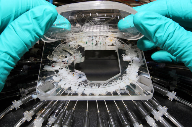
Figure 1. Vacuum manifold for securely connecting a microfluidic device to external inputs (Image: NIST)
When designing microfluidic chips for use with vacuum manifolds, locating connections near the sides will reduce the likelihood of the chip substrate bending due to compression force from the connectors. The density and size of microchannels makes the positional accuracy of these connections critical. Locating pins are frequently used in precision machining and are an excellent way to achieve rapid and precise positioning of chips as they are loaded into the system. A manifold design which allows XY compliance will help ensure that connections are made securely. Pairing a round alignment pin with a diamond shaped pin enables a small amount of rotation around the round pin. The long axis of the diamond pin (fig. 2) should be oriented perpendicular to the line between the center of the diamond pin and the round pin.
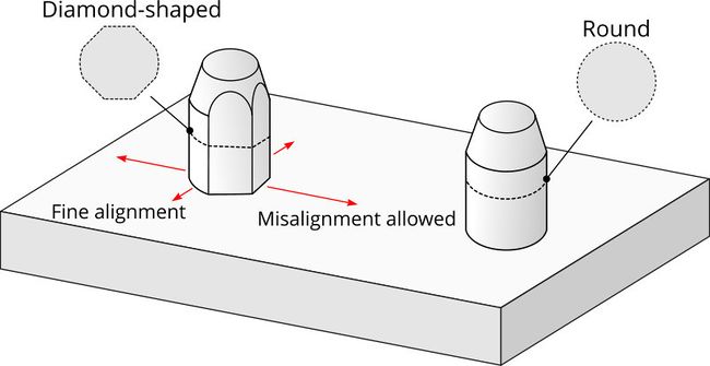
Figure 2. Providing XY compliance in the vacuum manifold to chip substrate mounting can help to ensure secure channel and electrical connections. A diamond-shaped alignment pin allows misalignment in one direction while providing fine alignment in the perpendicular direction.
Repeatable Chip Imaging
On many chips, the locations of channels and ports will not all be visible within the field of view of a high-power microscope objective, leading to difficulties in localizing images to match chip features when loading new samples.
Figure 2. Providing XY compliance in the vacuum manifold to chip substrate mounting can help to ensure secure channel and electrical connections. A diamond-shaped alignment pin allows misalignment in one direction while providing fine alignment in the perpendicular direction.
| Objective Magnification | Numerical Aperture | Field of View [um] | Depth of Field [um] |
|---|---|---|---|
| 40x | 0.65 | 540 | 1.05 |
| 50x | 0.75 | 432 | 0.78 |
| 63x | 0.75 | 343 | 0.77 |
| 100x | 0.85 | 216 | 0.59 |
Table 1. Example: BFS-U3-244S8M camera with 2.74um pixel size, 4/3” format (21.6mm diagonal). As magnification increases, the field of view and depth of field decrease, making it increasingly difficult to capture all key features with a single exposure.
One way to solve this issue is to use a motorized XY microscope stage such as Zaber’s X-ASR and X-ADR series. These stages, controlled by the Zaber Motion Library, are ideal building blocks for an automated positioning system for fresh chips. By scanning a fiducial mark on the chip, it is possible to localize and establish a datum for other features on the chip. Fiducials can also be conveniently used for serialization or identification of the chips when they are loaded into the imaging system.
Fiducial marks should be high-contrast and non-repeating features which are co-located with the microfluidic channels. Creating a fiducial directly on the chip by molding in a cross-shaped channel and infusing it with ink is a useful alternative to photomasked sputter coating. Printed stickers may also be used, however their precision is significantly less than on-chip features.
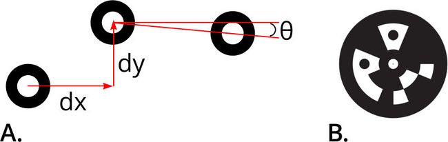
Figure 4. Example fiducial markers. These high contrast features are easily recognized by computer vision libraries and can be used to accurately compute position and orientation relative to the camera (A). Binary coded digital optical fiducial targets (B) contain additional information enabling computer vision systems to identify and differentiate between adjacent fiducials. Coded digital fiducials can enable systems to easily handle multiple configurations of microfluidic and maintain traceability of samples.
Example Microfluidic Positioning System
An example positioning system was built using a Nucleus® MVR inverted microscope. The Nucleus automated microscopy platform provides a complete set of interchangeable hardware modules and software tools for building a bespoke microscope such as the MVR inverted microscope. This example system combines chip positioning, illumination and focus control into a single easy to use device. Automation is achieved via the Python Zaber Motion Library API and the popular OpenCV computer vision library. Together these libraries enable the system to automatically find a fiducial marker and center it in the image frame by controlling an XY stage.
Detailed information on how to install Zaber Motion Library for Python available here. Detailed information on how to install OpenCV for Python is available here.
XY Chip Positioning Example

Figure 5. Examples of features which can be located and used for chip positioning.
First, a fiducial marker reference image is loaded and a connection to the motion control modules of the Zaber microscope is opened. The first position of the chip is an estimated rough location of the fiducial. Intentionally misaligning the initial position slightly down and to the left of the nominal position as shown in figure 6 (B) provides a known direction for the expected location of the fiducial.
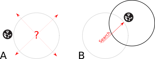
Figure 6: By intentionally misaligning the initial FOV (B) we can search in a known direction to find the fiducial.
SERIAL_PORT = "COM4"
ROUGH_POSITION = (25, 35)
FIDUCIAL_PATH = "fiducial.png"
def main():
   # Load the input image
   fiducial_reference = cv2.imread(FIDUCIAL_PATH)
   with Connection.open_serial_port(SERIAL_PORT) as connection:
       with Camera() as cam:  # Acquire and initialize Camera
           device_list = connection.detect_devices()
           device = device_list[4]
           focus = device_list[2].get_axis(1)
           axis_upper = device.get_axis(2)
           axis_lower = device.get_axis(1)
           axis_upper.move_absolute(ROUGH_POSITION[0], Units.LENGTH_MILLIMETRES)
           axis_lower.move_absolute(ROUGH_POSITION[1], Units.LENGTH_MILLIMETRES)
           # Initialize and trigger the Blackfly camera
           # Camera must be previously configured for software triggering
           cam.start()
           cam.TriggerSoftware()
           img = cam.get_array()
OpenCV template matching can then be used to find the position of the fiducial within the image. This assumes that the rotation and scale of the fiducial will be nearly the same as the template. If this is not the case, other more advanced methods such as FLANN descriptors can be used.
match_img = cv2.matchTemplate(grayscale_img.astype(np.float32), fiducial_reference, cv2.TM_CCOEFF_NORMED)
(minVal, maxVal, minLoc, maxLoc) = cv2.minMaxLoc(match)
if maxVal > threshold:
   found=cv2.rectangle(img,maxLoc,[sum(x) for x in zip(maxLoc,fiducial_reference.shape)],(255, 0, 0),5)
cv2.imshow('found',found)
If no fiducials are found, this process is repeated, searching up and to the right in small increments.
else:
   # Search with the requested stepsize
   axis_upper.move_relative(-xstep, Units.LENGTH_MILLIMETRES)
   axis_lower.move_relative(ystep, Units.LENGTH_MILLIMETRES)
Once a fiducial is found, compute the centroid and set it as the origin.
   # Compute the centroid and the distance from the center of the image
   centroid=(int(maxLoc[0]+fiducial_reference.shape[0]/2), int(maxLoc[1]+fiducial_reference.shape[1]/2))
   found = cv2.circle(found, centroid, 10, (255, 0, 0), 2)
   center_dist=(centroid[0]-img.shape[0]/2,img.shape[1]/2-centroid[1])
   return center_dist
   # Compute the origin and move to it
   origin=(axis_upper.get_position(Units.LENGTH_MICROMETRES)-pixel_calibration(pos[0]),axis_lower.get_position(Units.LENGTH_MICROMETRES)+pixel_calibration(pos[1]))
   axis_upper.move_absolute(origin[0],Units.LENGTH_MICROMETRES)
   axis_lower.move_absolute(origin[1],Units.LENGTH_MICROMETRES)
Channel Alignment with Theta Axis Example
Figure 7. Example of a motorized X-Y-theta microfluidic positioning system built using a Zaber ASR100 XY stage and a Zaber GSM goniometer stage.
While the XY scanning system above can solve many of the common problems with chip registration, it is limited to two degrees of freedom. In cases where secondary sensors must be aligned along the microfluidic channel, an additional theta axis is required. The previous XY chip alignment example can be expanded by adding a goniometer stage to rotate the chip and achieve precise channel alignment.
To measure the tilt of the sample, we then repeat the process at a second fiducial located on the other side of the sample. Using the difference between the known and measured separation between these marks we can compute the rotation of the sample and either correct for it or cancel it out using the theta axis.
   FIDUCIAL_OFFSET=(0.5)
   axis_upper.move_rel(FIDUCIAL_OFFSET)
   fid2=fiducial_search(0.98,0.05,0)
   # Compute the tilt of the sample
   theta=math.atan((fid2[1]-origin[1])/(fid2[0]-origin[0]))
Finally, the origin and homography that were measured are used to move to the target position on the chip.
   def move_homography(x,y,origin,theta):
   axis_lower.move_absolute(origin[0]+x+y/math.tan(theta),wait_until_idle=False)
   axis_upper.move_absolute(origin[1]+y+x*math.tan(theta),wait_until_idle=False)
   axis_upper.wait_until_idle()
   axis_lower.wait_until_idle()
One important consideration is that the chip's center of rotation will likely be slightly offset from the center of rotation of the stage. This means that an adjustment of rotation will be an iterative process, requiring correction of the center in XY as well.
Summary
Automated positioning of microfluidic chips to accurately align the world-to-chip interface and read its results can greatly improve the reliability and throughput of operations performed on-chip. While building an automated positioning system can be complex and time consuming, it doesn’t need to be! Zaber microscopes combine the key motion control and imaging elements into a single system. With Python scripting of the Zaber Motion Library and OpenCV, an automated chip positioning can be quickly implemented for chip alignment in two or three axes.